Starting from the single crystal rod produced in the single crystal furnace, the process flow of the wafer is basically started. In order to help everyone understand and understand the detailed production process of silicon materials to silicon wafers, and raise awareness of this industry so as to better engage in the photovoltaic industry, some production process data are now collated as follows, hoping to help everyone.
Introduction
The preparation of the silicon wafer begins with the silicon monocrystalline rod and ends with a clean polished wafer so that it can be used in an excellent environment. During the process, from a single crystal silicon rod to several wafers that can be processed to meet specific requirements, many processes and cleaning steps are required. In addition to many process steps, the entire process is almost carried out in a dust-free environment. The processing of silicon wafers began in a relatively dirty environment and was finally completed in a net vacant tenth inventory.
Process Overview
All the process steps are summarized in three main categories: the ability to correct physical properties such as size, shape, flatness, or the performance of some bulk materials; to reduce the amount of unwanted surface damage; or to eliminate surface contamination and particles. The order of the process steps is important because the decisions of these steps can cause the silicon wafer to suffer as little damage as possible and can reduce the contamination of the silicon wafer.
Wafer processing process steps
1. Slice
2. Laser marking
Chamfer
4. Grinding
5. Corrosion
6. Back injury
7. Edge mirror polishing
8. Preheat cleaning
9. Resistance to Stability - Annealing 10. Back Seal
11. Stickies
12. Polishing
13. Cleaning before inspection
14. Visual inspection
15. Metal cleaning
16. Brush
17. Laser inspection
18. Package/Freight
Slice (class 500k)
In the introduction of wafer processing, the first step starting from a single crystal silicon rod is slicing. The key to this step is how to reduce losses as much as possible when processing monocrystalline silicon rods into silicon wafers. This means that the single crystal rods must be processed as much as possible into useful silicon wafers. In order to get the best silicon wafers as possible, the wafers require a minimum amount of warpage and a minimal amount of kerf loss.
There are two main methods in the slicing process - internal circular cutting and wire cutting. The reason that these two types of cutting methods are applied is that they can minimize material loss, have minimal damage to the silicon wafer, and allow the warpage of the silicon wafer to also be minimal.
Slicing is a relatively dirty process that can be described as a grinding process that produces a large number of particles and a lot of very shallow surface damage.
After the wafer is cut, the sticky carbon plate and the adhesive used to stick the carbon must be removed from the wafer. During this cleaning and cleaning process, it is important to maintain the order of the wafers, because at this time they have not been identified.
Laser Marking (Class 500k)
After the boule has been cut into wafers, the wafer is laser engraved. A high-power laser printer is used to mark the silicon surface. The silicon wafer is coded in the same order as it was cut from the ingot so that the correct position of the wafer can be known. This code should be uniform and used to identify the silicon and know its source. The code can indicate from which position of the single crystal rod the silicon wafer is cut. Maintaining such traceability is important because the overall properties of the single crystal will vary from one end to the other of the crystal rod. The number needs to be deep enough so that the final wafer can be held after polishing. After engraving the code on the silicon chip, even if the silicon chip is missing, it can be traced back to the original position, and if it is clear, then correct measures can be taken. The laser marking can be on the front side of the silicon wafer or on the back side, although the front side is usually used.
Chamfer
When the slicing is completed, the wafer has sharp edges and chamfering is required to form bullet-like smooth edges. The chamfered wafer edge has a low center stress and therefore makes it stronger. This silicon wafer edge enhancement can reduce the silicon wafer fragmentation during subsequent wafer processing.
Grinding (Class 500k)
The next step is to remove the different damages that occur during the slicing process and laser marking. This is done during the slicing process. In the chipping, the silicon wafer is placed on the carrier and placed around some of the grinding discs. Both sides of the wafer can be in contact with the disc so that both sides of the wafer can be ground simultaneously. The disc is made of cast iron and has a jagged edge. There is a series of holes in the upper grinding disc that allow the grinding sand to be distributed on the silicon wafer and moved along with the grinding machine. Grinding can remove the serious damage caused by slicing, leaving only a few balanced, shallow scars. The second advantage of swarf is that after grinding, the wafer is very smooth because the disc is extremely flat.
The grinding process is mainly a mechanical process. The grinding disk oppresses the grinding sand on the surface of the silicon wafer. The abrasive sand consists of fine particles formed by delaying the calcination of the alumina solution, which grinds the outer layer of silicon. The depth of the outer layer to be ground is deeper than the depth of the damage caused by the slice.
Corrosion (Class 100k)
After grinding, there is a certain amount of balanced damage on the surface of the silicon wafer. These damages are removed but additional damage is caused as low as possible. More distinctive is the use of chemical methods. There are two basic corrosion methods: alkaline and acid corrosion.
Back Injury (Class 100k)
The mechanical damage on the back of the silicon wafer is to form a metal gettering center. When the silicon reaches a certain temperature, metal atoms, such as Fe, Ni, Cr, Zn, etc., which will reduce the lifetime of carriers will move in the silicon body. When these atoms encounter damage points on the back of the wafer, they are trapped and instinctively move from the inside to the point of damage. The introduction of back injuries is typically through impact or abrasion. For example, the impact method is grit blasting, and the abrasion is rubbed with a brush on the surface of the silicon wafer.
Edge polishing
The purpose of polishing the edge of the silicon wafer is to remove the etching pit left on the wafer edge. When the edge of the wafer becomes smooth, the stress on the edge of the silicon wafer becomes even. The even distribution of stress makes the silicon more robust. The polished edge minimizes the adsorption of particulate dust. The polishing method at the edge of the silicon wafer is similar to the polishing of the silicon wafer surface.
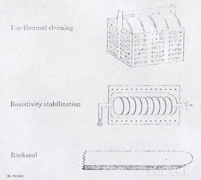
Preheat Cleaning (Class 1k)
Before the silicon wafer enters resistance stability, it needs to be cleaned to remove the organic matter and metal contamination. If there is metal remaining on the surface of the silicon wafer, when it enters the resistance stabilization process and the temperature rises, it will enter the silicon body. The cleaning process here is to immerse the silicon wafer in a cleaning solution (H2SO4+H2O2) capable of removing organics and oxides. Many of the metals will be dissolved as an oxide in the chemical cleaning solution; then, hydrofluoric acid (HF) will be used. The oxide layer on the surface of the silicon dissolves to remove dirt.
Resistance Stability - Annealing (Class 1k)
The silicon wafer grows in a high concentration of oxygen in a CZ furnace. Because most of the oxygen is inert, there is still a small amount of oxygen that forms small groups. These groups will play the role of n-donors, which will make the silicon wafer's resistivity test incorrect. To prevent this problem from occurring, the silicon wafer must first be heated to about 650°C. This high temperature causes oxygen to form large groups without affecting the resistivity. The silicon wafer is then quenched to prevent the formation of small oxygen radicals. This process can effectively eliminate the oxygen as an n-donor and stabilize the true resistivity.
Back Seal (Class 10k)
For heavily doped silicon wafers, a high temperature stage is used to deposit a thin film on the backside of the wafer, which prevents outdiffusion of dopants. This layer acts as a sealant to prevent the escape of dopants. There are three types of thin films that are commonly used as back-sealing materials: silicon dioxide (SiO2), silicon nitride (Si3N4), and polysilicon.
The figure illustrates the steps of preheat cleaning, resistance to stabilization, and back sealing.
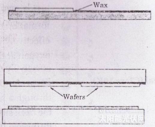
Stickies (Class 10k)
Before polishing, the adhesive sheet must be applied first. The adhesive sheet must ensure that the wafer can be polished flat. There are two main types of adhesives, namely wax or template adhesives.
The wax adhesive sheet is bonded to the silicon wafer with a solid rosin wax and provides an extremely flat reference surface. This surface provides a solid reference plane for polishing. The sticky wax prevents the movement of the wafer when the wafer is polished under a carrier on one side. Wax sticks are useful only for single-sided polished silicon wafers.
Another method is a template patch, with two different variations. One is only suitable for single-side polishing. In this way, the silicon wafer is fixed on a round template and placed on a soft liner. This pad provides enough friction so that when polishing, the edge of the wafer does not fully support the side carrier and the wafer does not hard contact but "floats" on the object. When polished on the front, the single-sided adhesive sheet protects the backside of the silicon wafer. Another method is suitable for double-sided polishing. This method can allow polishing on one machine, both sides can be performed at the same time, and the operation is similar to the machine. The two polishing pads of the silicon wafer are placed in opposite directions so that the silicon wafers are pushed toward the top of one direction and the bottom of the opposite direction, and the resulting stresses cancel each other out. This helps prevent the silicon wafer from being pushed into a hard carrier and causing damage to the wafer edge.
Polishing (Class ≤ 1k)
The purpose of silicon wafer polishing is to obtain a very smooth, smooth, non-damaged silicon surface. When grinding, the silicon wafer is mechanically ground; when it is polished, it is a chemical/mechanical process. This difference in the principle of operation is responsible for the fact that polishing can produce a smoother surface than the pad.
During polishing, silicon wafers are chemically/ mechanically polished with special polishing pads and special polishing sands. Polished sand consists of silica gel and a special high-pH chemical reagent. This high-pH chemical agent acts on the surface of the silicon oxide sheet and mechanically polishes the oxide layer from the surface with silica-containing polishing sand.
Wafers are usually polished in multiple steps. The first step is rough polishing. With a harder liner, the polishing sand reacts more easily, and there are more rough silica particles than the sand used in the subsequent polishing. The first step is to remove the corrosion spot and some mechanical damage. In the following polishing, a soft lining, polished sand containing less chemical reagents and fine silica gel particles was used. The final polish that removes remaining damage and mist is called fine polishing.
The adhesive sheet and polishing process are as shown in the figure:
Pre-inspection cleaning (class 10)
After the wafer is polished, there is a lot of contaminants on the surface. In order to be able to inspect the silicon, it is necessary to clean it to remove most of the particles. Through this cleaning, the cleanliness of silicon wafers still cannot meet the requirements of customers, but they can be checked.
The usual cleaning method is to use RCA SC-1 cleaning solution after polishing. Sometimes when cleaning with SC-1, it is more effective to use magnetic ultrasonic cleaning. Another method is to use H2SO4/H2O2, then HF cleaning. In contrast, this method is more effective in removing metal contamination.
an examination
After polishing, cleaning, you can check it. During the inspection process, the resistivity, warpage, total thickness overshoot and flatness must be tested. All these measurement parameters are tested in a non-contact method so that the polished surface is not damaged. At this point, the silicon wafer must eventually meet the customer's dimensional performance requirements, or it will be eliminated.
Metal removal cleaning
After the wafer is inspected, a final cleaning is performed to remove all particles remaining on the surface of the wafer. The main contaminants are the metal ions that remain on the surface of the wafer after cleaning before inspection. These metal ions come from various processes that use metal and silicon wafers, such as slicing and grinding. Some of the metal ions even come from the chemicals used in the previous cleaning process. Therefore, the final cleaning is mainly to remove metal ions remaining on the surface of the silicon wafer. The reason for this is that metal ions can cause minority carrier lifetimes, which can degrade device performance. The SC-1 standard cleaning solution is not very effective at removing metal ions. Therefore, different cleaning solutions, such as HCl, must be used.
Wipe
After cleaning the wafer with HCl, some particles may also be adsorbed on the surface. Some manufacturers choose PVA brushes to remove these residual particles. In the scrubbing process, pure water or ammonia (NH4OH) should flow through the surface of the wafer to remove the attached particles. Rubbing with PVA is an effective way to remove particles.
Laser inspection
After the final cleaning of the silicon wafer is completed, the surface particles and surface defects need to be inspected. The laser tester can detect surface particles and defects. Because the laser is a high-intensity wave source in short waves. The laser reflects on the silicon surface. If there is no problem with the surface, the light hits the surface of the wafer and reflects at the same angle. However, if the light hits the particles or hits a rough surface, the light will not reflect at the same angle. The reflected light travels in all directions and can be detected at different angles.
Packaging/freight
The purpose of the package is to provide a dust-free environment for the silicon wafers and to protect the silicon wafers from any damage while they are being transported; the package also prevents the silicon wafers from getting wet. If a good piece of silicon is placed in a container and contaminated with it, its degree of contamination will be as severe as at any stage in the processing of the wafer, or even considered as a more serious problem because of the production of silicon wafers. During the process, with the completion of each step, the value of silicon is also rising. The ideal package is to provide both a clean environment and a neat and tidy environment for storage and transportation. Typical shipping containers are made of polypropylene, polyethylene, or some other plastic material. These plastics should not release any gas and be dust-free, so that the surface of the silicon wafer will not be contaminated.
Silicon wafer preparation stage
In the manufacturing process of silicon wafers, many parameters are involved. And many of these parameters will change depending on the final silicon target. For silicon wafers, there are some parameters that are always important, such as flatness, defects, contamination, and so on.
When the wafer is cut by an incorrectly operating blade, it will create a curved edge. These blades will not be the same. This will cause the wafer to have different kinds of plane defects. Therefore, the silicon wafer should be cut as flat as possible.
There are different measurement methods to test the flatness of the wafer. The entire flatness is very important for the design of samples. On the other hand, the local flatness is important for the design. Some terms of overall flatness testing are the bow and warp. , TTV, TIR, and FPA.
Silicon wafer preparation stage
There are many parameters involved in the manufacturing of silicon wafers. And many of these parameters will change depending on the final silicon target. For silicon wafers, there are some parameters that are always important, such as flatness, defects, contamination, and so on.
When the wafer is cut by an incorrectly operating blade, it will create a curved edge. These blades will not be the same. This will cause the wafer to have different kinds of plane defects. Therefore, the silicon wafer should be cut as flat as possible.
There are different measurement methods to test the flatness of the wafer. The entire flatness is very important for the design of samples. On the other hand, the local flatness is important for the design. Some terms of overall flatness testing are the bow and warp. , TTV, TIR, and FPA.
Bow:
Wafer bending is a measurement of the degree of bending of the silicon wafer, which is the degree of deviation from the center of the wafer from a plane that is established by three base points near the edge of the wafer.
Warp:
Another test method for deformation of the silicon wafer shape is the warpage test. The degree of warpage is the maximum difference between the highest point and the lowest point of the centerline position of several reference planes defined by the silicon wafer. Wafer warpage depends on the use of a pair of non-contact scanning probes. The silicon wafer is placed on three fulcrums that form the reference plane. One of the pair of probes can be anywhere on one side of the wafer and the other is in the corresponding position on the other side. The probe moves along the surface of the wafer according to a set procedure and measures the distance to a specified point on the surface of the wafer. Once all the distances have been measured, the degree of warping will be known. To determine the degree of warpage, the first step is to find the distance between the top probe and the top silicon surface (a) and the distance between the bottom probe and the bottom silicon surface (b). In other words, all the measurement points of ba are obtained. With these data, the ba value is subtracted from the ba value, and divided by 2 is the Warp value (shown in Figure 1.6).
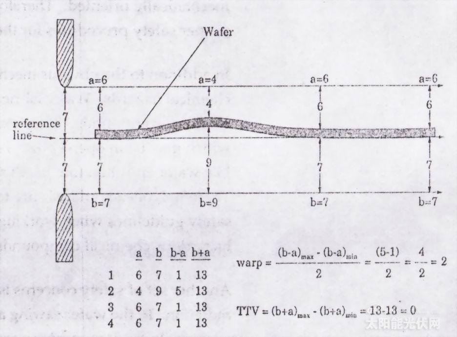
Figure 1.6 Warp and Total Thickness Deviation (TTV) Measurements
TTV
A method of detecting the consistency of the thickness of a silicon wafer, which is called the total thickness overshoot (TTV), is the difference between the maximum and the minimum thickness of the silicon wafer. Measurement TTV can be performed simultaneously while measuring Warp. Similar probes and data processing methods in Warp can be used by TTV. When calculating TTV, the first step is to add the distance (a) between the top probe and the top silicon surface and the distance (b) between the bottom probe and the bottom silicon surface. Here, we want to add ( a+b), TTV is to subtract the minimum value of a+b from the maximum value of a+b.
TIR
The total indicator reading is a parameter that relates only to the front side of the wafer. The measurement method is to use the side suctioned in parallel with the vacuum chuck as the reference plane, and the TIR is the difference between the top and bottom of the front. (See Figure 1.7)
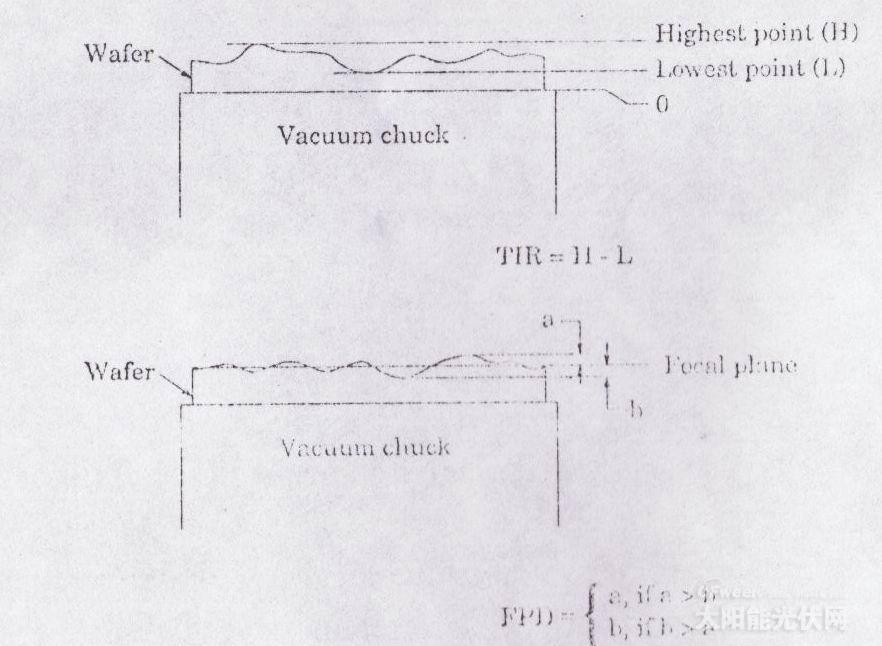
Figure 1.7 Total Indicating Reading (TIR) ​​and Focal Plane Deviation (FPD) Measurements
FPD
The focal plane deviation (FPD) is the distance from the highest point of the focal plane and the farthest to the focal plane of the wafer. All test methods reflect the overall surface condition of the silicon wafer.
Pollution
The contamination of the silicon surface is a major concern. The wafer production process begins with relatively dirty chips and ends with a net vacancy. The wafers are exposed to a large number of different chemicals and solutions, and the wafers are placed in many different machines for machining. Both of these contacts can cause particle contamination. The other two major pollutions are metals and organics. Metals Because silicon wafers are machined in many machines, metals are held in contact with the surface of the silicon wafer and remain on the surface of the silicon wafer; organic materials may come from grease or oil on any object. All contamination must be removed before the silicon is finally sent to the customer.
Safety
In the wafer manufacturing stage of semiconductor manufacturing, many safety issues are very similar to those in a well-equipped equipment store, with high-speed blades and all hand-rolling equipment. Many processes in silicon wafer production are mechanically oriented. Therefore, these dangerous processes must have certain safety procedures.
Chemical hazards: The production of silicon wafers requires the use of many dangerous chemicals, such as HF and KOH used in open silicon wafer cleaning. The use of these chemicals is as frequent as water, and it is easy to instill a false sense of security. Therefore, when working with these chemicals, all correct safety policies must be determined.
There are other safety issues related to various radiations. In the slice area, there is an X-ray source; in the laser scanning area, the radiation of the laser may cause a potential fire and even blindness. In these areas, appropriate protective clothing should be worn and care should be taken to prevent safety problems.
Glossary
Bow:
Wafer bending refers to the degree of departure from the center of the wafer to a plane created by the three base points near the edge of the wafer. The degree of curvature is for the entire wafer.
Level 10 (class10):
Generally referring to the cleanliness of the environment, Level 10 refers to no more than 10 particles of 0.5 μm in size per cubic foot of air and a greater number of particles. This is a very clean environment.
Silica gel:
A suspended silica particle that is too fine to distinguish individual particles and cannot be separated from the suspension.
Micro-cut:
It is caused by the quivering of the blade, which is the slight deviation of the blade during travel, and the tiny ridge damage left on the silicon chip along the cut.
Outside suction:
This is a gettering method that is suitable for use on the backside of silicon wafers.
Focal plane deviation (FPD):
The focal plane away from the test can indicate the furthest distance from the focal plane at any point on the front side of the wafer. The FPD can measure the entire surface of the silicon wafer.
Getter:
It is a method to induce metal impurities away from the front of the silicon wafer.
Atomization:
It is a condition of the fog on the silicon wafer. May be caused by any contamination or damage to the silicon wafer.
Average carrier lifetime: refers to the average recombination time of majority carriers in silicon.
Piranha:
It is a cleaning solution composed of sulfuric acid (H2SO4) and hydrogen peroxide (H2O2). The reason for this name is because when the above two chemicals are mixed, the temperature of the solution will reach about 120°C and it will boil violently.
Total indicator reading (TIR):
It is the distance between the highest point and the most concave point on the front surface of the silicon wafer. TIR can indicate the front of the entire wafer.
Total thickness difference (TTV):
This refers to the difference between the thickest and thinnest areas of the silicon wafer. TTV is also a test of the entire wafer.
Warp:
It refers to the difference between the highest and lowest distances from the centerline of the wafer. It is the test of the entire wafer.

Key Specifications/Special Features:
High performance Ferrite Magnet
Used for dish-washer pumps, Wash Machine Pumps, Aquarium pumps, Pond Pumps
With big quantity existing mould
Various size and shape available
OD: from 9mm~40mm
Application: Wash Machine Pump, Dishwasher Pump, Aquarium Pump, Pond Pump

Cylinder Ferrite Magnet,Ferrite Magnet Cylinder Magnet ,Strong Cylinder Ferrite Magnets,Cylinder Shaped Ferrite Magnets
Chongqing Great Well Magnet Co.,ltd. , https://www.gwmagnet.com